Electron Microscope
What is it?
Advantages and Disadvantages
The Electron Microscope (EM) is an impressively powerful microscope that exists today, allowing researchers to view a specimen at nanometer size.
History - Ernst Ruska
Ernst Ruska (1906-1988), a German engineer and academic professor, built the first Electron Microscope in 1931, and the same principles behind his prototype still govern modern EMs.

While studying under Dr. Max Knoll at the technical university of Munich, he became interested in the possibility of electron microscopy as a solution to the limitations of optical or light microscopes.
Ruska understood that electron wavelengths are far shorter than light wavelengths and believed that, if he could find a way to apply this knowledge, he could develop a far more powerful microscope.
Together with Knolls, he developed the first electromagnetic lens, which focused a beam of electrons in lieu of an illuminator onto a source to create a magnified image.
Although this early version did not offer significant improvements to the optical microscope, Ruska was able to modify the electron lens and develop a more powerful version in the late 1930s.
He later worked as an electrical engineer for the Siemans Company, which manufactured the first electron microscope.
Ruska was awarded the Nobel Prize for Physics in 1986, credited with one of the most influential innovations of the 20th century.
Electron Microscopy
An EM is a microscope that focuses beams of energetic electrons to examine objects up to nano-scales.
They utilize the same principles behind an optical microscope, but rather than photons or particles of light, concentrate electrons, charged particles located on the outside of atoms, onto an object.
Additional differences include preparation of specimens before being placed in the vacuum chamber, the use of coiled electromagnets instead of glass lenses, the use of a thermionic gun as an electron source and the image or electron micrograph is viewed on a screen rather than an eyepiece.
All EMs use electromagnetic and/or electrostatic lenses, which consist of a coil of wire wrapped around the outside of a tube, commonly referred to as a solenoid.
In addition, EMs use digital displays, computer interfaces, software for image analysis and a low vacuum or variable pressure chamber, which upholds the pressure differential between the high vacuum levels essential to the gun and column area and the low pressure required in the chamber.
All electron microscopy samples must be prepared before placed in the microscope vacuum.
Techniques, which vary based on type of specimen and analysis, include:
- Cryofixation
- Fixation
- Dehydration
- Embedding
- Sectioning
- Staining
- Freeze-fracture and Freeze-etch
- Sputter Coating
Most of these techniques require specialized training and, due to sample manipulation, can result in artifacts or inadvertent changes to the structure of the specimen.
Experienced researchers may be able to differentiate actual sample properties from artifacts, but there is no absolute way to identify all potential artifacts on every single sample.
Nanoscale Imaging

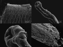
Pictured right - Electron microscope details of hair; a cut strand a root the tip of the root and a worn end.
In this microscope, images are produced from the interaction between the prepared samples in the vacuum chamber and energetic electrons.
The electron beam passes through one or more solenoids and, with the aid of the thermionic electron gun, is directed down the column and onto the sample.
Equivalent to the magnification that occurs from light refraction in an optical microscope, the coils in an EM bend the electron beams to create an image.
Any changes to the electromagnetic wavelength will effect the movement of the electrons; for example, if you increase the voltage of the accelerating electron beam, you will increase the image resolution.
When the energetic electrons come in contact with the sample, the reaction(s) provide information on topography or surface texture, morphology, which includes the size, shape and arrangement of detectable surface particles and the composition of elements and compounds as well as crystallographic information, which refers to the arrangement of atoms.
The following gives you a description of two types of EMs,the Transmission (TEM) and Scanning Electron Microscope(SEM).
Transmission Electron Microscopes
The transmission electron microscope (TEM), the first type of EM, has many commonalities with the optical microscope and is a powerful microscope, capable of producing images 1 nanometer in size.
They require high voltages to increase the acceleration speed of electrons, which, once they pass through the sample (transmission), increase the image resolution.
The 2-d, black and white images produced by TEMs can be seen on a screen or printed onto a photographic plate.
Although recent innovations in software help to minimize, TEM resolution is hampered by spherical and chromatic aberrations.
The TEM is a popular choice for nanotechnology as well as semiconductor analysis and production.
Scanning Electron Microscopes
Reflecting light microscopes are the optical counterpart to scanning electron microscopes (SEM) and produce similar data.
SEMs are primarily used to obtain topographical information.
In this type of EM, a series of solenoids pulls the beam back and forth across the sample, systematically scanning the surface; it detects secondary electrons emitted from the surface and produces an image.
Although SEMs are approximately 10 times less powerful than TEMs, they produce high-resolution, sharp, black and white 3D images.
Scroll down the following articles to learn more about Scanning Electron Microscopy pertaining to pollen and bone tissue.
Electron Microscope Advantages
The primary advantage is its powerful magnification.
The potential runs the gamut of scientific fields including biology, gemology, medical and forensic sciences, metallurgy and nanotechnologies.
EMs also have many technological and industrial applications, such as semiconductor inspection, computer chip manufacturing, quality control and can even be used as part of a production line.
Electron Microscope Disadvantages
The main disadvantages are cost, size, maintenance, researcher training and image artifacts resulting from specimen preparation.
This type of microscope is a large, cumbersome, expensive piece of equipment, extremely sensitive to vibration and external magnetic fields.
It needs to be kept in an area large enough to contain the microscope as well as protect and avoid any unintended influence on the electrons.
Upkeep involves maintaining stable voltage supplies, currents to electromagnetic coils/lens and circulation of cool water so the samples are not damaged or destroyed from heat given off during the process of energizing the electrons.
Special training is required to learn the involved processes of specimen preparation, to minimize and recognize preparation-related artifacts and to operate the microscope itself.
Despite these disadvantages, EMs are assets to high-end research laboratories; this powerful piece of equipment has resulted in innumerable advances in science and industry.
Considered by many to be one of the finest scientific innovations, the electron microscope is a powerful imaging tool surpassed only by the atomic force microscope.
EMs focus beams of energetic electrons onto a sample to produce high-resolution images, detailing such characteristics as surface structure, texture, size and composition.
The Transmission Electron Microscopes and Scanning Electron Microscopes have practical applications in such fields as biology, chemistry, gemology, metallurgy and industry as well as provide information on the topography, morphology, composition and crystallographic data of samples.
Check out a great page on Nanotechnology here
Scanning (SEM) - Learn about the SEMs high-resolution, three-dimensional images which provide topographical, morphological and compositional information making them invaluable in a variety of science and industry applications.
Transmission (TEM) - check out one of the most powerful microscopic tools available to-date, capable of producing high-resolution, detailed images 1 nanometer in size.
Cryo-Electron - is a type of transmission electron microscopy that allows for the specimen of interest to be viewed at cryogenic temperatures. Check it out.
Virtual - provides a simulated microscope experience via a computer program or Internet website for both educational and industrial applications and are easily operated and accessible.
Take a look at how Electron Microscopy compares to Super-Resolution Microscopy.
Taking a look at Viruses under the Microscope and answering the question, what are viruses?
As well as Atom under the Microscope and DNA under the Microscope
Electron microscopy (SEM and TEM) images of SARS-CoV-2 - Covid 19
What is Near Field Scanning Optical Microscopy?
Return from Electron Microscope to Best Microscope Home
Find out how to advertise on MicroscopeMaster!


